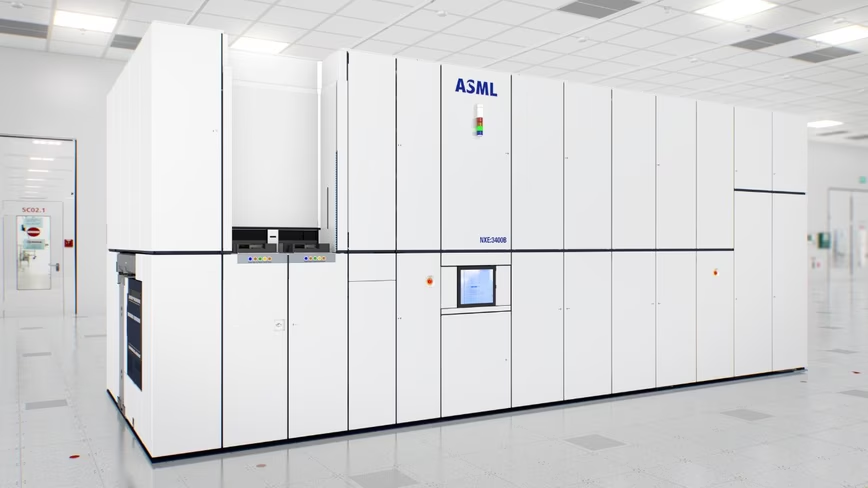
ASML, the sole producer of chipmaking machines used in the world’s most advanced semiconductors, has opened a test lab for its High NA EUV lithography equipment, its most high-end tool to date.
The laboratory, located in Veldhoven, the Netherlands, is a joint venture between ASML and Belgian chip research company imec. It will provide leading chipmakers and other materials and equipment suppliers with early access to the High NA EUV prototype scanner.
The High NA machines represent the latest advancement in extreme ultraviolet (EUV) lithography systems, which use light to draw chip patterns on the silicon wafer.
According to ASML, these machines can manufacture faster, smaller, and more energy-efficient chips. They reportedly come with a €350mn price tag — compared to the price of €200mn for the company’s regular EUV tools.
To date, only Intel has secured access to the High NA machines. But now the lab will enable ASML’s customers and partners to access the technology before the system is available at their own factories.
“This type of very early engagement with the ecosystem is unique,” ASML’s President and CEO Christopher Fouquet said in a statement.
“[It] could significantly accelerate the learning curve on the technology and smoothen the introduction in manufacturing.”
The Dutch chip giant expects the lab to support the de-risking of the technology, before the tools are operational for high-volume manufacturing in 2025-2026.
For imec, the laboratory will work as a virtual extension of its 300mm cleanroom for Complementary Metal Oxide Semiconductor (CMOS) technology in Leuven, on which it’s also collaborating with ASML.
Meanwhile immec, which is a key player in Europe’s chip sector, has secured €2.5bn to host a separate pilot line of sub-2 nanometre chips, with use cases spanning from healthcare to automotive applications.
Now, the joint lab with ASML aims to provide unprecedented access to testing the most advanced semiconductor technology currently available, while retaining R&D expertise in Europe.
Get the TNW newsletter
Get the most important tech news in your inbox each week.


