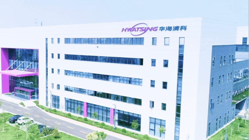
Hwatsing, China headquarters
 Credit: Hwatsing
Hwatsing Technology, China’s leading producer of chemical mechanical polishing equipment, announced a metrology system for six-inch wafers on Thursday that can be built directly into the polishing workflow. The company describes it as China’s first six-inch metrology system paired with CMP equipment.
The integration is the substantive part. Rather than measuring wafers separately after processing, the system takes readings before and after polishing and feeds live data back to the control system, according to the South China Morning Post.
Why polishing matters more than it sounds
Chemical mechanical polishing flattens and smooths the silicon disc between processing layers. Modern chips stack dozens of layers, and each one has to be planar to within nanometres or the next layer prints badly.
It is unglamorous work that determines yield. Closing the measurement loop should improve wafer uniformity and cut waste, which matters more in a country whose fabs run older lithography and need every point of yield they can find.
The number in the announcement
Six inches is 150mm. Leading-edge logic runs on 300mm wafers, and the sub-10nm nodes that export controls exist to restrict are made nowhere else.
The 150mm format belongs to mature nodes and compound semiconductors, and even there it is being left behind. Silicon carbide power devices are already migrating from 150mm to 200mm in volume manufacturing, while gallium nitride is moving from 200mm towards 300mm.
None of that makes the tool unimportant. It does mean this is a step on a ladder rather than a jump to the top of it.
What Hwatsing has actually achieved
The company’s track record is the stronger signal. China’s share of the global CMP equipment market rose from roughly 1.5% in 2022 to almost 11% in 2023, with Hwatsing responsible for most of the gain, according to Georgetown’s Center for Security and Emerging Technology.
Volume backs that up. Hwatsing shipped its 1,000th CMP system in April and has said it is targeting advanced chip manufacturing next.
It is spending accordingly, seeking up to 4 billion yuan, around $552 million, through a private placement to expand capacity, build out wafer reclamation services, and fund high-end tool development. A separate $237 million plant investment is also underway.
Applied Materials still leads the CMP market decisively, with Ebara holding roughly 27% globally. Eleven percent is a real position, not a dominant one.
The lithography problem it does not solve
Polishing tools are not the binding constraint. ASML remains the only company making EUV lithography machines, and China cannot buy them at any price under US-led export controls.
That is where the more consequential work is happening. China’s homegrown immersion DUV tool now has a name, Shanghai Aishengna, and a domestic DUV machine would matter considerably more than a metrology upgrade, though independent analysts have attached heavy caveats to reported progress there.
The strategy underneath
Beijing’s approach is to close every gap it can while the hardest one stays shut. Chinese semiconductor equipment self-sufficiency has reportedly reached around 35%, up from roughly 25% two years earlier.
Washington is weighing further restrictions on chip equipment sales, with Beijing arguing that cutting the supply chain damages everyone in it. Each round of controls has accelerated the localisation it was meant to prevent.
What success looks like when it arrives
China has already proved it can build a world-scale chip company in a segment where the tools are obtainable. Memory maker CXMT jumped 466% on its Shanghai debut to become the most valuable listed DRAM company in the country.
Demand is following. Apple has begun testing CXMT memory chips, which is roughly the highest-profile validation a Chinese chipmaker can receive.
CXMT still depends on foreign equipment it cannot always get. That is precisely the dependency tools like Hwatsing’s are meant to unwind, one process step at a time, which is slower than a breakthrough but harder to sanction.
Get the TNW newsletter
Get the most important tech news in your inbox each week.


